
I am exploring this cool simulator online, https://edaplayground.com/. It can be helpful for programming FPGAs.
Let’s make a Ramp Wave:
So the general idea is simple. There is a clock going into the FPGA. The code simple counts every time the clock tics. And then you are turning that into an output.
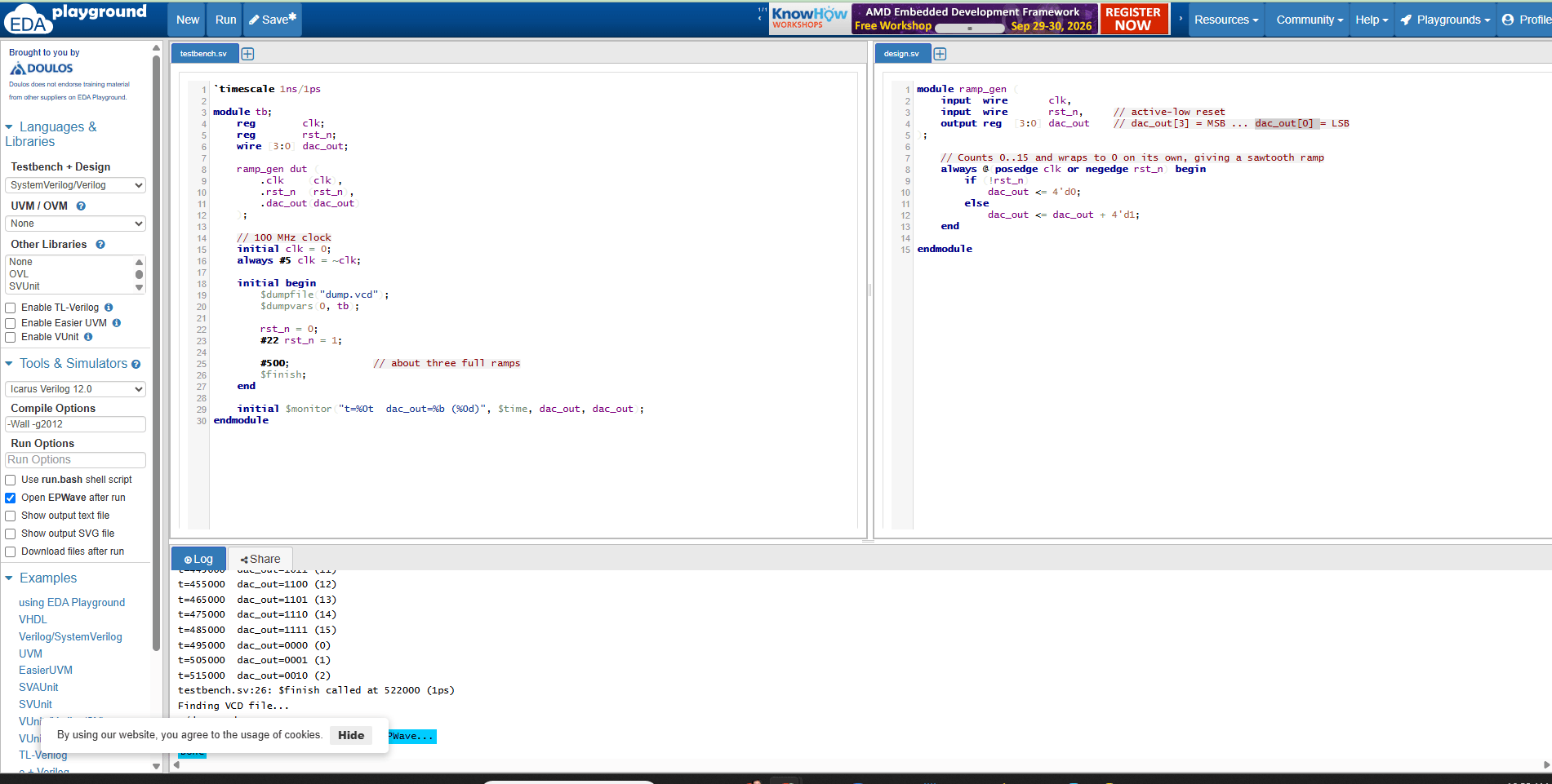
Note: I had to select Icarus
Here are some questions I have for Claude:
>> dac_out[0] refers to one of the outputs on the FPGA board? Does dac_out[1] refer to another?Yes, but only once you assign them to pins. In the code, dac_out is a 4-bit bus, and dac_out[0], dac_out[1], dac_out[2], and dac_out[3] are four separate signals. Each one becomes its own output pin on the FPGA, so each drives its own resistor in the ladder.The code itself doesn't say which physical pins they are. You do that in a constraints file when you build for a real board. In Xilinx/Vivado (XDC), for example, it looks like this:set_property PACKAGE_PIN J1 [get_ports {dac_out[0]}]set_property PACKAGE_PIN J2 [get_ports {dac_out[1]}]set_property PACKAGE_PIN J3 [get_ports {dac_out[2]}]set_property PACKAGE_PIN J4 [get_ports {dac_out[3]}]set_property IOSTANDARD LVCMOS33 [get_ports {dac_out[*]}]Those pin names (J1 to J4) are made up. On your board you'd pick four free pins, such as a Pmod header, and use the names from the board's manual or master constraints file. Intel/Altera boards use a .qsf file for the same job, and Lattice uses an .lpf or .pcf.The bit order matters for the ladder. dac_out[0] is the LSB and should go to the end of the ladder with the extra 2R to ground. dac_out[3] is the MSB and goes closest to the output node. If you swap them, the ramp comes out scrambled instead of smooth.EDA Playground only simulates. There is no board, so dac_out[0] through dac_out[3] are just waveforms in EPWave. The pin assignment only comes into play when you move the design into a vendor tool like Vivado or Quartus and program a real board.Which board are you planning to use? I can write the exact constraints for it.
Here’s a few more:
>> So the module ramp_gen in the design function basically is telling you what the output would be?Almost. The module doesn't just tell you what the output would be, it is the description of the circuit that produces the output.ramp_gen describes hardware: a 4-bit register that gets +1 on every clock edge, with a reset that sends it back to zero. When you simulate it, the simulator behaves like that hardware would and shows you the resulting values of dac_out. When you synthesize it for an FPGA, the tool turns the same description into actual flip-flops and adder logic inside the chip, and the four bits come out on the pins you assigned.
>> The testbench file is what actually runs the code?Not quite. The simulator runs both files together. It compiles the design and the testbench, then starts the simulation from the testbench's top-level module (tb in this case).The testbench is what drives the simulation, though, so it's the reason anything happens. The design is like a circuit with nothing plugged into it. On its own, ramp_gen has no clock and no reset, so it would just sit there doing nothing. The testbench creates the clock, releases reset, and sets how long the simulation runs before $finish. Inside it, the line ramp_gen dut (...) places your design as a component and wires it up.So the flow on EDA Playground is:You click Run.The simulator compiles both files.It starts at tb, the top level.tb generates the clock and reset, and the ramp_gen inside it responds to them.The waveforms are recorded, and EPWave shows them.Both files are needed: the testbench supplies the stimulus, and the design supplies the behavior being tested.
>> What does "always #5 clk = ~clk;" do

That line generates the clock. Reading it left to right:

always means "repeat this forever," starting at time zero.
#5 is a delay of 5 time units. With timescale 1ns/1ps at the top of the testbench, that's 5 ns.
clk = ~clk; inverts the clock, so 0 becomes 1 and 1 becomes 0.

Put together: wait 5 ns, flip the clock, wait 5 ns, flip it again, and so on forever.

That's why the line above it matters: initial clk = 0; sets the starting value. Without it, clk begins as x (unknown), and inverting an unknown gives another unknown, so the clock would never toggle.

The timeline looks like this:

Time	clk
0 ns	0
5 ns	1
10 ns	0
15 ns	1

Each flip takes 5 ns, so a full cycle (low then high) takes 10 ns, which is 100 MHz. The rising edges at 5, 15, 25 ns and so on are what trigger always @(posedge clk ...) in your design, and each one steps the counter up by one.

To change the speed, change the delay. #50 gives a 100 ns period (10 MHz), and #1 gives a 2 ns period (500 MHz). The period is always twice the number after the #.

This is testbench-only code. The # delay has no hardware equivalent, so on a real board the clock comes from an oscillator on the board instead.
SO THIS IS IMPORTANT! Don’t include this when you are running the real code because the time is set by the board.
>> So the initial begin module wouldn't be needed for a physical system?Right. The initial begin ... end block in the testbench is simulation-only, so it doesn't go on a physical system. It's part of the testbench, which never becomes hardware.Here's what each piece of it does and what replaces it on a real board:$dumpfile / $dumpvars: record waveforms to a file. On hardware there's nothing to record; you'd look at the pins with a scope or logic analyzer instead.rst_n = 0; #22 rst_n = 1;: holds reset low, then releases it after 22 ns. On a board, reset usually comes from a push button or a power-on reset circuit.#500; $finish;: stops the simulation. Hardware doesn't stop; it just runs until you cut power.$monitor: prints values to the console. There's no console on the chip.The same goes for the clock: always #5 clk = ~clk; is replaced by the board's oscillator.One caveat on initial blocks: they aren't always simulation-only. Some FPGA tools accept a small initial block inside a design module to set a register's starting value (for example, initial dac_out = 0;), and they turn it into the flip-flop's power-up value. That's a tool-specific convenience. Your ramp_gen doesn't use one; it relies on the reset input instead, which is the more portable approach.So for the physical build, you'd take only ramp_gen, add a constraints file for the pins, and connect the clock and reset inputs to the board's oscillator and a button.
Now let’s get the arbitrary waveform part.
>> so Ramp waves seem easy? What about other shapes? What if we wanted to make a waveform of a different mathematical function? Let's x^3Designing a lookup-table approach for a DAC waveform generator.Designing a lookup-table approach for a DAC waveform generator.Ramp waves are easy because a counter already counts in a straight line. For any other shape, you put a step between the counter and the DAC that turns the count into the function's value. The usual way is a lookup table (a small ROM): the counter is x, the table holds f(x), and the table's output drives the ladder.For x³ on a 4-bit DAC, x runs 0 to 15, so x³ runs 0 to 3375. You have to scale that down to fit 0 to 15, so each table entry is round(x³ × 15 / 3375), which is round(x³ / 225).design.sv (replaces the old one; the testbench works unchanged since the ports are the same)verilogmodule ramp_gen ( input wire clk, input wire rst_n, output reg [3:0] dac_out); reg [3:0] x; // the counter, now internal always @(posedge clk or negedge rst_n) begin if (!rst_n) begin x <= 4'd0; dac_out <= 4'd0; end else begin x <= x + 4'd1; // dac_out = round(x^3 / 225), scaled to fit 0..15 case (x) 4'd0: dac_out <= 4'd0; 4'd1: dac_out <= 4'd0; 4'd2: dac_out <= 4'd0; 4'd3: dac_out <= 4'd0; 4'd4: dac_out <= 4'd0; 4'd5: dac_out <= 4'd1; 4'd6: dac_out <= 4'd1; 4'd7: dac_out <= 4'd2; 4'd8: dac_out <= 4'd2; 4'd9: dac_out <= 4'd3; 4'd10: dac_out <= 4'd4; 4'd11: dac_out <= 4'd6; 4'd12: dac_out <= 4'd8; 4'd13: dac_out <= 4'd10; 4'd14: dac_out <= 4'd12; 4'd15: dac_out <= 4'd15; endcase end endendmoduleIn EPWave you'll see the staircase stay flat near zero, then curve upward faster and faster, which is the cubic shape.The limit with 4 bits. The first five outputs are all 0, because x³ is tiny for small x and a 4-bit output can't show that detail. The curve looks coarse. To get a smoother one you need more resolution:a wider DAC (8 bits means 256 output levels and a much smoother curve)more table entries (say a 6-bit counter, so 64 points along the curve)Table vs. calculating. You could compute x*x*x directly in Verilog, and synthesis tools will build a multiplier for it. The table is usually simpler and works for any function, including ones that are awkward to compute like sine, since you just fill in the values ahead of time. It's the standard way to generate sine waves on FPGAs. Tools typically map a table like this onto block RAM or logic.If you want a more classic cubic look, I can shift it so x runs from -8 to +7. Then the curve is an S-shape that flattens through the middle instead of only rising.
Okay this make sense now.
The magic is happening in this block of code:
                4'd0:  dac_out <= 4'd0;
                4'd1:  dac_out <= 4'd0;
                4'd2:  dac_out <= 4'd0;
                4'd3:  dac_out <= 4'd0;
                4'd4:  dac_out <= 4'd0;
                4'd5:  dac_out <= 4'd1;
                4'd6:  dac_out <= 4'd1;
                4'd7:  dac_out <= 4'd2;
                4'd8:  dac_out <= 4'd2;
                4'd9:  dac_out <= 4'd3;
                4'd10: dac_out <= 4'd4;
                4'd11: dac_out <= 4'd6;
                4'd12: dac_out <= 4'd8;
                4'd13: dac_out <= 4'd10;
                4'd14: dac_out <= 4'd12;
                4'd15: dac_out <= 4'd15;
Let’s think about the function f(x) = x^3. What are the values.
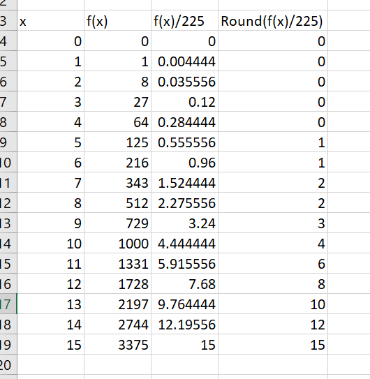
Let’s walk through the logic.
x is a number from 0 to 15
x^3 goes from 0 to 3375
But the max output of our DAC is 15. So we 3375 / 15 = 225. So to properly scale our function we need to divide by 225.
For the final step we need to round our data because we can only generate 0s and 1s. Remember that 1111 = 15. (https://cosmicpathways.org/2026/09/22/quick-explanation-of-r2r/)
So that basically means to make an arbitrary shape, we need to generate these values for our function. So what would that look like in python? if we wanted to generate some function x^2 til 8 then 0:
import numpy as npimport matplotlib.pyplot as plt### Simple code for generating an aribrary shapebits = 4Steps = bits**2 # bits ^2#Make Functionx = np.arange(Steps)y = x**2mask = x > 8y[mask] = 0plt.plot(x,y,'o')plt.xlabel ("x")plt.ylabel ("y")
Which would have the following output
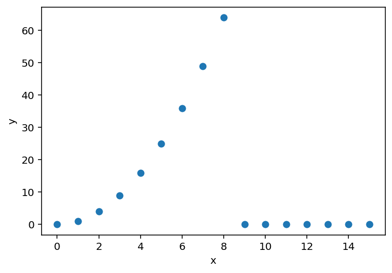
Remember the make value can only be 15 or bits**2-1, so we have to normalize the function. So this would like:
import numpy as npimport matplotlib.pyplot as plt### Simple code for generating an aribrary shapebits = 4Steps = bits**2 # bits ^2#Make Functionx = np.arange(Steps)y = x**2mask = x > 8y[mask] = 0TopValue = max(y)NormValue = TopValue / (Steps-1)y = y / NormValue #normalize yplt.plot(x,y,'o')plt.xlabel ("x")plt.ylabel ("y")
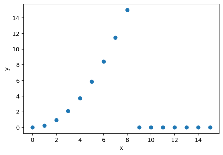
Notice now this only goes to 15
import numpy as npimport matplotlib.pyplot as plt### Simple code for generating an aribrary shapebits = 4Steps = bits**2 # bits ^2#Make Functionx = np.arange(Steps)y = x**2mask = x > 8y[mask] = 0TopValue = max(y)NormValue = TopValue / (Steps-1)y = y / NormValue #normalize yy = np.round(y) #round yplt.plot(x,y,'o')plt.xlabel ("x")plt.ylabel ("y")
Now let’s print it out. We loop through each value. put the x output on the left. Put the updated y output on the right. Now that numpy python wanted y to be a floating point number. I forced it into an integer with int command.
import numpy as npimport matplotlib.pyplot as plt### Simple code for generating an aribrary shapebits = 4Steps = bits**2 # bits ^2#Make Functionx = np.arange(Steps)y = x**2mask = x > 8y[mask] = 0TopValue = max(y)NormValue = TopValue / (Steps-1)y = y / NormValue #normalize yy = np.round(y) #round yplt.plot(x,y,'o')plt.xlabel ("x")plt.ylabel ("y")for ii in range(Steps): #Build output string Part1 = "4'd" + str(ii) Part2 = ": dac_out <= 4'd" + str(int(y[ii])) + ";" hld = Part1 + Part2 print (hld)
The output looks like this:
4'd0: dac_out <= 4'd0;4'd1: dac_out <= 4'd0;4'd2: dac_out <= 4'd1;4'd3: dac_out <= 4'd2;4'd4: dac_out <= 4'd4;4'd5: dac_out <= 4'd6;4'd6: dac_out <= 4'd8;4'd7: dac_out <= 4'd11;4'd8: dac_out <= 4'd15;4'd9: dac_out <= 4'd0;4'd10: dac_out <= 4'd0;4'd11: dac_out <= 4'd0;4'd12: dac_out <= 4'd0;4'd13: dac_out <= 4'd0;4'd14: dac_out <= 4'd0;4'd15: dac_out <= 4'd0;
And Claude now says:
so this will compile once it sits inside the case (x) block of the design. Here is the full file with your table dropped in:verilogmodule ramp_gen ( input wire clk, input wire rst_n, output reg [3:0] dac_out); reg [3:0] x; always @(posedge clk or negedge rst_n) begin if (!rst_n) begin x <= 4'd0; dac_out <= 4'd0; end else begin x <= x + 4'd1; case (x) 4'd0: dac_out <= 4'd0; 4'd1: dac_out <= 4'd0; 4'd2: dac_out <= 4'd1; 4'd3: dac_out <= 4'd2; 4'd4: dac_out <= 4'd4; 4'd5: dac_out <= 4'd6; 4'd6: dac_out <= 4'd8; 4'd7: dac_out <= 4'd11; 4'd8: dac_out <= 4'd15; 4'd9: dac_out <= 4'd0; 4'd10: dac_out <= 4'd0; 4'd11: dac_out <= 4'd0; 4'd12: dac_out <= 4'd0; 4'd13: dac_out <= 4'd0; 4'd14: dac_out <= 4'd0; 4'd15: dac_out <= 4'd0; default: dac_out <= 4'd0; endcase end endendmoduleSince all 16 values of the 4-bit x are listed, the default line will never actually trigger. It's harmless, and it keeps some tools from warning about an incomplete case.Use the same testbench as before with no changes. In EPWave, dac_out should step up through 0, 0, 1, 2, 4, 6, 8, 11, 15, then drop to 0 for seven clocks, and repeat every 16 clocks (160 ns). The output lags the counter by one clock, so the first cycle looks shifted slightly.To see it as a curve rather than a row of numbers, right-click dac_out in EPWave and choose the analog display option.If you'd like the curve to use the whole 16-step cycle instead of dropping to zero halfway, I can give you a table for that.



Leave a Reply